In VLSI design, what is VLSI Front end and what is VLSI Back end ? What does a front end engineer do compared to a back end engineer in the vlsi design flow ? Who has better opportunities in terms of career and earning potential? These are some common questions that every student or an entry level engineer encounters.
Introduction:
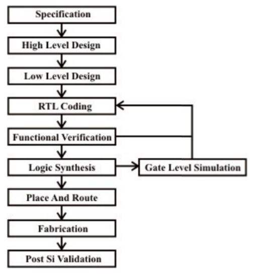
Lets try to understand this in detail. Following diagram illustrates a standard VLSI Design life cycle and the various stages involved in a design from specification to manufacturing.

-
- Specification: This is the first stage in the design process where we define the important parameters of the system that has to be designed into a specification.
- High level Design: In this stage, various details of the design architecture are defined. In this stage, details about the different functional blocks and the interface communication protocols between them etc. are defined.
- Low level Design: This phase is also known as microarchitecture phase. In this phase lower level design details about each functional block implementation are designed. This can include details like modules, state machines, counters, MUXes, decoders, internal registers etc.
- RTL coding: In RTL coding phase, the micro design is modelled in a Hardware Description Language like Verilog/VHDL, using synthesizable constructs of the language. Synthesizable constructs are used so that the RTL model can be input to a synthesis tool to map the design to actual gate level implementation later.
- Functional Verification: Functional Verification is the process of verifying the functional characteristics of the design by generating different input stimulus and checking for correct behavior of the design implementation.
- Logic Synthesis: Synthesis is the process in which a synthesis tool like design compiler takes in the RTL, target technology, and constraints as inputs and maps the RTL to target technology primitives. Functional equivalence checks are also done after synthesis to check for equivalence between the input RTL model and the output gate level model.
- Placement and Routing: Gate-level netlist from the synthesis tool is taken and imported into place and route tool in the Verilog netlist format. All the gates and flip-flops are placed, Clock tree synthesis and reset is routed. After this each block is routed, output of the P&R tool is a GDS file, which is used by a foundry for fabricating the ASIC
- Gate level Simulation: The Placement and Routing tool generates an SDF (Standard Delay File) that contains timing information of the gates. This is back annotated along with gate level netlist and some functional patterns are run to verify the design functionality. A static timing analysis tool like Prime time can also be used for performing static timing analysis checks
- Fabrication: Once the gate level simulations verify the functional correctness of the gate level design after the Placement and Routing phase, then the design is ready for manufacturing. The final GDS file (a binary database file format which is the default industry standard for data exchange of integrated circuit or IC layout artwork) is normally send to a foundry which fabricates the silicon. Once fabricated, proper packaging is done and the chip is made ready for testing.
- Post silicon Validation: Once the chip is back from fabrication, it needs to be put in a real test environment and tested before it can be used widely in the market. This phase involves testing in lab using real hardware boards and software/firmware that programs the chip. Since the speed of simulation with RTL is very slow compared to testing in lab with real silicon, there is always a possibility to find a bug in silicon validation and hence this is very important before qualifying the design for a market.
The set of above stages are roughly divided into two halves – the first half is known as Front end of VLSI design while the second half is referred to as Back end VLSI design.
Front End VLSI Design: All of the stages from Specification to Functional Verification are normally considered as part of Front end and engineers working on any of these are Front end VLSI design engineers.
Back End VLSI Design: All stages from Logic Synthesis till Fabrication are considered as back end and engineers working on any of these are considered as Back end VLSI design engineers.
Some job categories though have some vague distinction between front end vs back end:
- Post Silicon validation is normally a separate phase for product readiness. Some times engineers working on this have more interactions with front end design and verification engineers.
- Emulation , FPGA design and PCB design are also not truly classified in this design flow.
- Gate level simulation is mostly done my front end VLSI design engineers even though it is post synthesis
- There are also separate job categories like Custom circuit design, Analog and Mixed signal circuit designs – which could be considered separate.
Career Opportunities – Front end vs Back End:
In terms of opportunities and importance, both Front end engineers and Back end Engineers are equally important, equally challenged. Both will have equal opportunities in terms of building a career and opportunities to earn.
On the front end side, an engineer could start as an RTL design engineer or a Verification engineer and gain deeper knowledge and skills as they progress in career. In terms of job opportunities, there is demand for more verification engineers compared to design engineers.
Engineers could gain deeper knowledge and expertise in same domain. Some engineers who have strong interest in architecture and microarchitecture can also grow as system design architects and microarchitects.
On the back end side, engineers can start with logic synthesis, Placement and Routing , Layout, Physical verification, static timing analysis. Most of the back end engineers would need a better understanding of process technologies, transistors, high speed design issues and a good grasp of tools and automation.
An engineer can choose to have a career in front end or back end based on these understanding and their specific interest and skills. In terms of earning opportunity, both have equal opportunities and beyond the differentiation – a lot would depend on how you learn, execute and grow.
Also read my following related blog posts
- Opportunities for Electronics Engineers
- Verification, Validation and Testing of SOCs – Differences
- What are skills needed for Chip design engineers
- Verification Engineers – Opportunities and Career path
Further if you have any question related to VLSI design or career, feel free to check out my answers or ask a new one on Quora – Ask a Question on My Quora

